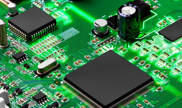
Printed Circuit Board – an overview
The layout and production of a circuit board is a step-by-step manner: schematic creation and simulation, putting in PCB design grids and DRCs, component placement, PCB routing, power planes, and sooner or later assembling the BOM and building the board. The next degree of design will focus on these steps.
How to Make a Printed Circuit Board
Although the design and manufacturing of a PCB may be generalized as schematic seize, PCB layout, and circuit board fabrication and meeting, the information of each step are very involved. We’ll take a look right here at some of the more particular elements of each of these steps.
Create the Schematic
Before starting the design of the board inside the CAD tools, it is important to ensure that the library component designs are completed. PCB Manufacturer For the schematic, this means developing common sense symbols for the parts so that it will be carried out; resistors, capacitors, inductors, connectors, and integrated circuits (ICs).
With these components ready to be used, begin by means of organizing them on schematic sheets within the CAD gear. Once the components are roughly located, wires can be drawn that constitute the connectivity between the pins of the schematic symbols. These strains are known as nets, and they can represent unmarried nets or agencies of nets for reminiscence or data circuits. During the schematic seize, process components must be moved as had to create a schematic that is legible and clean.
Simulate the Circuitry
With parts and nets prepared on the schematic, the next step is to verify that the circuit will work the intended way. To verify this, hire circuit simulations in a simulation program with the Integrated Circuit Emphasis tool, otherwise called SPICE. These equipment allow PCB engineers to test the circuits they may be designing before building the actual hardware. As such, they are able to store money and time, making those tools an critical a part of the PCB design system.
CAD Tool Setup
The design equipment that PCB designers use have many distinct abilties, consisting of the ability to installation layout regulations and constraints to be able to maintain distinct nets from overlapping at the same time as retaining the appropriate quantity of distance to exclusive gadgets. There are more than one extra aids to be had to the clothier, consisting of design grids that can assist to location additives and direction lines in a neat and orderly way.
Layout Components
With your layout database installation successfully and the net connectivity records imported from the schematic, the bodily format of the circuit board is the next assignment. The first step is to area the component footprints in the board define within the CAD device. Each footprint will have the internet connections displayed as a “ghost-line” picture to show the fashion designer which parts they connect with. Placing these elements for their great overall performance whilst being aware of connectivity, areas of immoderate warmness and electric noise, and different physical obstructions which include connectors, cables, and mounting hardware is a mission that designers will advantage with enjoy. The needs of the circuit alone are not the only constraining aspect: designers must consider placing the additives so they can be high-quality assembled with the aid of the manufacturer.